Slide thumbnail

4th ePIXfab Silicon Photonics

Design Course

11-15 April 2022, Ghent University (Belgium)

Slide thumbnail

Here you learn to make

your own

silicon photonics chips

What is covered in the course?

The Specialist Course on Silicon Photonics Design goes from ideation to characterization of a working silicon photonics chip.

The course focuses on the process to translate a photonic circuit idea into a working chip, going from schematic design and circuit simulation to layout, routing, and interactive design rule checking.

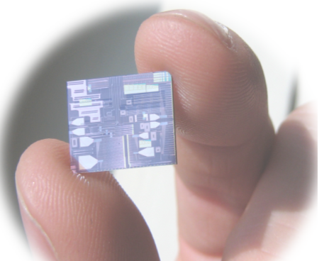
As part of the course, the participants get the opportunity to actually tape out a design that will be fabricated with an e-beam prototyping service and characterized. Based on these results, the design can be improved and submitted to a wafer-scale multi-project-wafer run of which the participants will receive the final chips.

Who can benefit from it?

The hands-on course is designed for researchers and engineers with a fundamental understanding of photonic integrated circuits.

Key features of the course

Achieve mastery in silicon photonics integrated circuit design

Full coverage of circuits, components, simulation, layout, tape-outs, …

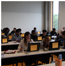
Five days hands-on design lab going all the way from idea to PIC

Get your silicon photonics design fabricated and have it characterized

Practical information

Course Instructor

Prof. Wim Bogaerts
Prof. Wim BogaertsGhent University - imec, Belgium

Content of the course

From:9 AM to 12.30 PM

Topics
Introduction to the course
Introduction to photonic ICs and silicon photonics
Quick start: Photonic Circuit design
Hands-on: Basics of Jupyter notebooks, Python
Hands-on: Constructing circuits

From 13:30 PM to 17:00 PM

Topics
Design flow of silicon Photonic ICs
Introducing the tape-outs and PDKs
Hands-on: Exploring the PDKs and the PICAZZO library
Hands-on: Setting up the project
Hands-on: Building blocks
Australian Silicon Photonics

From 9:00 PM to 12:30 PM

Topics
Waveguides and building blocks
Hands-on: Waveguides: dispersion, non-linearity , sensitivity
Hands-on: Directional couplers and other building blocks

From 13:30 AM to 17:00 PM

Topics
Component design and electromagnetic simulation
Hands-on: component designs, simulations and optimizations

Evening Activity (Food provided – subject to COVID conditions)

  • Using Lean techniques in a Fabless environment
  • Hands-on: Playing the “Fab game”

From 09:00 AM to 12:30 PM

Topics
Parametric cells (PCells) and custom layout
Circuit simulation and models (frequency domain and time domain)
Hands-on: Circuit simulation
Hands-on: PCells , Layout and Models

From 1:30 AM to 5:00 PM

Topics
Optical Wavelength Filters: Interferometers, AWGs, Echelle gratings and Rings
Hands-on: Wavelength filters

Evening Activity (Food provided – subject to COVID conditions)

  • Organizing your design flows and teams
  • Design of Experiment
  • Hands-on – Idea-generation for project designs

From 09:00 AM to 12:30 PM

Topics
Understanding the CMOS Process flow (for photonics)
Hands-on: Design Rule Checking

From 1:30 AM to 4:00 PM

Topics
Design for Manufacturability
Variability and parasitics
Hands-on: Tape-out process and design verification
Hands-on: Photonic parasitics
Hands-on: Variability analysis

After 16:30:

  • Visit to the “Castle of the Counts” (Subject to conditions)

18:30 onwards:

  • The Last Supper

From 09:00 AM to 12:30 PM

Topics
The Silicon Photonics ecosystem and Applications
Hands-on: Project Work and Exercises

From 1:30 AM to 5:00 PM

Topics
Analysis of measurement data
Hands-on: Data analysis and parameter extraction
Present your project idea
Wrap up

Detailed program: DOWNLOAD

Organized by

Supported by