
About Soitec
Soitec is a world leader in designing and manufacturing innovative semiconductor materials. With Slot Online than 3,500 active patents worldwide, Soitec’s strategy is based on disruptive innovation to answer customers’ needs for high performance, energy efficient and cost competitive engineered substrates.
Soitec offers a wide range of technologies and material engineering expertise which provide the electronics industry with new opportunities for innovation and differentiation. For photonics, our substrates are used as a reference for silicon photonics in particular for datacom, automotive, or healthcare applications.Soitec has manufacturing facilities, R&D centers and offices in Europe, the U.S. and Asia.
Expertise
SOI-based photonics substrates provided by SOITEC take advantage of the atomically flat and uniform Silicon crystalline layer enabling light routing through sub-micrometer-scale optical waveguides at appropriate wavelengths. Optical transceivers makers leverage this unique technology for datacenters interconnects(DCI). Based on its solid manufacturing process, SOITEC is the right partner for your business from R&D to high volume.
New applications are leveraging the amount of SOI demands becoming the future engine of many products in the next years for various segments such as Lidar, healthcare, HPC, Ai…

Why Photonics-SOI wafers from SOITEC benefits to Silicon optics ?
At infrared wavelength (> 1.1 µm), the crystalline silicon becomes transparent. Designers can then pattern this thin layer to obtain sub-micrometer-scale optical waveguides, while the oxide upper and under claddings provide strong optical confinement to route light on a chip in a tiny form factor.
Moreover, the high-index contrast of silicon-on-insulator (SOI) materials allows in small footprints the whole silicon photonics toolbox such as laser integration, input/output (I/O) couplers, high-speed modulators, photo detector and wavelength multiplexers.
SOI features are extensively engineered to go beyond standard pluggable transceivers, targeting a silicon photonics-silicon electronics monolithical co-integration, with optical chiplets surrounding CMOS high-demanding processors.
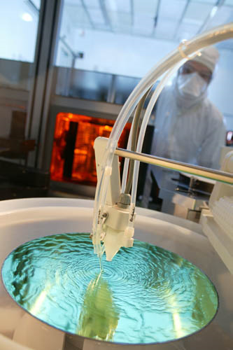
Wafers are available in 200mm and 300mm. As a leader in this category, Soitec wafers are used in the top end foundries.