About CEA-LETI
CEA is a French Governmental Research Organisation (15000 employees) devoted to both fundamental and Industrial Research & Development.
Within CEA, CEA-LETI is one of the major European research centers for applied electronics. It is located in Grenoble where it operates 11000 m²-State-of-the-Art CMOS clean rooms, 200 and 300 mm wafer size, and the 200 mm MEMS microsystems platform, with equipment worth some 200 M€. Nearly 1,600 men and women are serving innovation and the transfer of technology in key domains.
As a pioneer in Research & Development in Silicon Photonics (2002) CEA-Leti has developed strong expertise and know-how in devices’ design, integration and test, including Ge-on-Silicon photodetectors and heterogeneous III/V-on-Silicon lasers.
Expertise
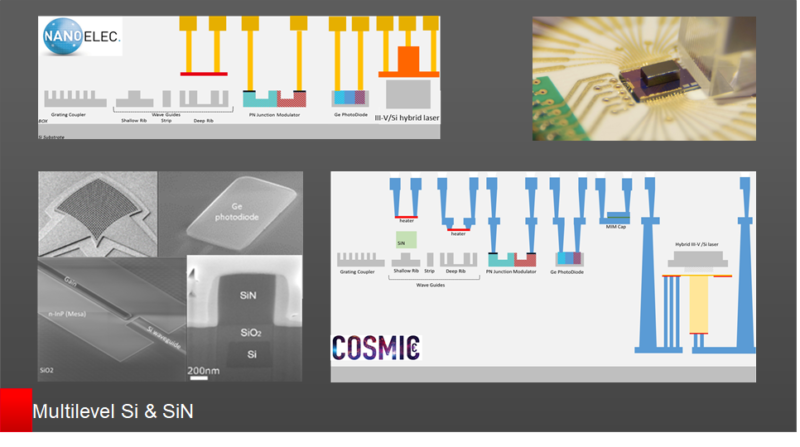
A. VERSATILE SI-SIN PHOTONICS PLATFORM
CEA-Leti’s versatile Si-SiN photonics platform allows miniaturization, power efficiency, cost reduction and scalability of photonic integrated circuits (PIC) from visible to mid-infrared.
CEA-Leti’s versatile Si-SiN photonics platform offers a broad range of CMOS compatible processes on 200 mm and 300 mm wafers that leverage world-class pre-industrialization equipment. This platform also offers the integration of amorphous Si, SiGe, Ge and SiN layers, and III-V-bonded epi layers on the same wafer, providing the advantages of each material.
Pioneering silicon photonics for more than 15 years, CEA-Leti has designed a technology toolbox with a device library of passive and active components featuring state-of-the-art performance for communication, computing and optical sensing.
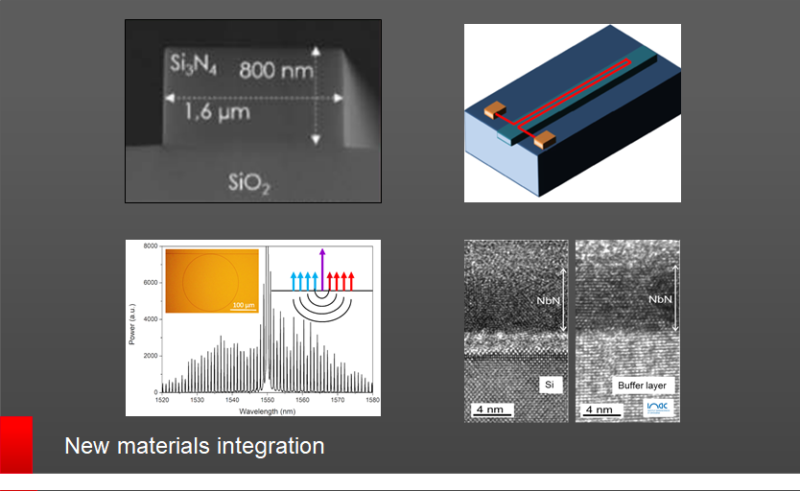
B. NEW MATERIALS INTEGRATION ON SILICON PHOTONICS PLATFORM
CEA-Leti’s photonics platform is very flexible and allows integration of new materials such as ultra-low loss SiN (ULL-SiN), NbN, and Phase Change Material (PCM) for high-speed interconnect, quantum and neuromorphic devices for 5G, secured com network, and AI applications.
Performances obtained with an 800 nm thick ULL SiN layer include a two-x reduction in propagation loss with 3 dB/meter for high-confinement 1.6 µm wide strip waveguides across S, C, and L optical-wavelength bands. High-Q photonic micro-resonators with quality factors approaching 107 across C-band are reachable.
CEA-Leti also develops the deposition of NbN on Silicon for high-efficiency NbN superconducting single-photon detector (SSPD) with improved NbN crystallinity and increased critical temperature.