ePIXfab represented European Silicon Photonics stakeholders at the world technology road mapping forum organized by
Photon Delta
.
Stakeholders within the silicon photonics community met in the Netherlands with the objective to make a comprehensive roadmap for integrated photonic technologies and applications for a short and long term time frame. Contributions from the whole PIC community and ePIXfab members in particular are highly welcome. Therefore, if you have an interest in contributing, feel free to mention your interest to us.
European Photonic Integration Forum 2017 organized by JePPIX and ePIXfab is a one-day event taking place on September 18th 2017 as part of the ECOC conference in Gothenburg, Sweden.
VPIphotonics is conducting, in cooperation with PhoeniX Software, a training on the computer-aided design of complex photonic components and integrated circuits. Date: 9-12 October, in Berlin, Germany.
The IEEE Photonics Benelux Chapter Annual Symposium 2017 will take place on 27-28 November 2017, Congress Center TU Delft. Abstract deadline has passed, speakers will be announced soon.
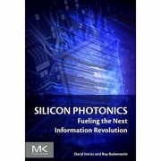
Editor’s pick: “Silicon Photonics: Fueling the Next Information Revolution”
This book, written by Inniss and Rubenstein, outlines the history and status of silicon photonics and discusses the trends driving the datacom and telecom industries.
It captures the latest research assessing silicon photonics development and prospects, demonstrates how silicon photonics addresses the challenges of managing bandwidth over distance and within systems, and explores potential applications, including servers, datacenters, and Internet of Things. For industry, but also for academia to widen their scope.
1.-5. October in Orlando, USA. This year with dedicated sessions on silicon photonics, photonic integration on silicon as well as several sessions on various aspects of photonics integrated circuits in general. Post-deadline paper submission is 26. September.
ECOC exhibition/conference offers an exciting and comprehensive coverage of cutting-edge basic and applied research and the newest developments in the field of optical communications and networking. It showcases state of the art results, which bridge the gap between basic science and applications.
Paper deadlines have passed, but registration is now open. Gothenburg, Sweden from 18-20 September 2017.
The 3rd edition of the Photonic Integration Conference will take place on September 26, 2017 at High Tech Campus Eindhoven, The Netherlands. This one-day conference offers insights on applications and current state of the integrated photonics industry, presented mainly by industry managers within the field.
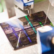
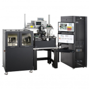
VTT acquires a wafer-level test system to support the production of silicon photonics
VTT
has acquired a system from SemiProbe to perform automatic and simultaneous electro-optical tests at wafer level.
This system supports research and production activities at VTT and at VTT Memsfab Ltd, providing contact manufacturing services for the 3 µm SOI technology platform. The system is able to handle 2 full cassettes (25 wafers each) of 150 or 200mm wafers and offers unmanned operation overnight. Test data are automatically acquired in customer-specified formats. In 2018 the goal is to test >1 million chips at wafer level while ramping up the manufacturing volume.
LIGENTEC and VLC collaborate to offer silicon nitride platform
One of the leading providers of manufacturing foundry services in silicon nitride
LIGENTEC
and the pioneering design house
VLC Photonics
team up to offer prototyping and production of photonic integrated circuits on silicon nitride. Dedicated full-wafer runs or shared multi-project wafer runs are offered three times a year and a PDK has been implemented for OptoDesigner by PhoeniX Software and IPKISS by Luceda Photonics.
With CORNERSTONE a new fabrication service for active and passive silicon photonic devices is now available in the UK. The team headed by Professor Graham Reed aims to offer up to four passive and two active calls per year. CORNERSTONE can offer both an industry compatible fabrication service, and design flexibility essential for research and prototyping purposes.
TowerJazz announced a new silicon photonics process, which complements its SiGe BiCMOS processes, utilized for the manufacturing of optical transceiver electronics. A collaboration with Phoenix Software provides customers with photonic PDKs for the manufacturing of photonic integrated circuits for optical networking components.
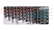
Researchers from MIT and Sherbrooke experimentally demonstrated an essential part of a new architecture for a fully optical neural network, using a programmable nanophotonic processor. It features a cascaded array of 56 programmable Mach–Zehnder interferometers in a silicon photonic integrated circuit and shows its use for vowel recognition.
Ultrahigh-Q Nanocavities Ready For Commercial Applications
Japanese researchers around Ashida et al. fabricated ultrahigh-Q photonic nanocavities with a record breaking Q value of 2.2 million, using standard CMOS technologies. This opens up the door for commercial applications of ultrahigh-Q nanocavities, such as nanocavity Raman silicon lasers.
The Center for Nanoscience and Nanotechnology (France), STMicroelectronics (France) and National Research Council (Canada) have recently demonstrated fiber-to-chip surface silicon grating couplers with radiation efficiency in the upwards direction exceeding 95% without the need for bottom mirrors.