Tutorial Topics & Abstracts

Download the detailed program of the school: DETAILED PROGRAM 

Note: This is a tentative program and the actual lecture order may change.
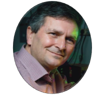
Introduction to silicon photonics

by

Prof. Roel Baets,

Ghent University – imec, Belgium

This lecture will provide holistic coverage of the field of silicon photonics. It will go from the early years of silicon photonics to how it has evolved over the years. The basic concepts, as well as the applications, will be touched upon in this lecture.

Debriefing: Passive silicon photonics: from basics to circuits

by
Prof. Andrea Melloni

Politecnico di Milano, Italy

The lecture provides a panorama of the potentials and limits of the silicon photonic platform to implement passive functionalities. Aspects apparently trivial or negligible that can have a large impact on the overall performance of the entire circuit will be considered with detail. The state of the art of passive devices will be shown and rings resonators will be treated in detail, starting from an historical survey and going through theory and applications. Several arguments have the scope to trigger further interests and are propaedeutic to the other lectures.

Debriefing: Laser integration in silicon photonics

by

Prof. Gunther Roelkens

Ghent University – imec, Belgium

In this lecture we will discuss the different methods (flip-chip, die-to-wafer bonding, transfer printing, monolithic integration) to integrate III-V semiconductor lasers and semiconductor optical amplifiers on silicon and silicon nitride waveguide circuits.

High-speed Modulators and Detectors in Silicon Photonics

by

Dr. Laurent Vivien

C2N, CNRS, Uni. Paris-Sud, Uni. Paris Saclay, France

Silicon photonics has been the subject of intense research activities as a compelling technology paving the way for next generation of energy-efficient high-speed computing, information processing and communications systems. The vision is to provide a mature integration platform supported by the CMOS manufacturing infrastructure to cost-effectively produce integrated optoelectronic circuits for a wide range of applications, including telecommunications, optical interconnects, spectroscopy, Quantum photonics, biological and chemical sensing…

This lecture will be focus on optical modulation in silicon photonics platform. Basic optical properties, state of the art, device integration, … will be introduced during the lecture as follows:

  • Light modulation in silicon platform
    • Physical effects and figures of merit
    • Experimental results
    • Trends in modulation

This lecture will be focus on the development of waveguide photodetectors in silicon photonics platform. Basic optical properties, state of the art, device integration, … will be introduced during the lecture as follows:

  • Light detection
    • Material choice
    • Properties
    • Experimental results
  • Conclusion and trends

Debriefing: Heterogeneous Integration for high-speed modulators in silicon photonics

by

Prof. Dries Van Thourhout

Ghent University-imec, Belgium

Modulators based on the carrier dispersion effect are readily available now from most standard silicon photonics platforms. They are very reliable and have been shown to enable high-speed data transmission.  However, there performance is fundamentally limited by the trade-off between modulation efficiency, losses and attainable bandwidth.  Therefore, the integration of novel materials, which could overcome these limitations, is widely investigated.  These is even more important for the SiN-platform, which has no native modulator.  In this talk I will first discuss the integration of Germanium and Graphene for realizing power-efficient electro-absorption modulators. Then I will discuss options for realizing pure phase modulators, such as the integration of Lithium Niobate, PZT or BTO using bonding, transfer-printing or different deposition processes.

Integrated Microwave Photonics

by
Prof. David Marpaung

University of Twente, the Netherlands

In this lecture I will discuss new technologies and paradigms underpinning the second-wave of integrated microwave photonics, including optical frequency combs, plasmonic modulators. programmable photonics, and photon-phonon interactions.

Silicon photonics ultrasound detection

by
Dr. Xavier Rottenberg

imec, Belgium

This lecture will introduce the basic concepts behind MEMS devices. We will focus on their electrostatic implementations and detail the working principle of Micromachined Ultrasound Transducers. This will form the basis for the further extension from electrostatic, piezoelectric or piezoresistive transduction to the implementation of sensors with integrated optical read-out. We will report on the development of integrated ultrasound microphones with application in acoustic and photo-acoustic imaging.

Machine learning and algorithm assisted design in silicon photonics

by

Prof. Dan-Xia Xu

National Research Council, Canada

Recent advances in nanophotonics are enabled by increased degrees of freedom in the device geometry and material parameters. Optimization algorithms and machine learning (ML) methods are increasingly applied to aid the exploration of immense design parameter spaces, encountered particularly in inverse design using parameterized or topological representations. We review some of the current trends and challenges in applying these methods to silicon photonics. We explore data-efficient machine learning methods such as dimensionality reduction for tackling complex design problems, and for multi-objective optimization.

Emerging applications of silicon photonics

by

Dr. Aaron Zilkie

Rockley Photonics, USA

The tutorial will cover three main areas, trends in Si Photonics for data communications including co-packaged optics, Si Photonics for FMCW automotive LiDAR, and Si Photonics for emerging consumer healthcare monitoring applications.

Programmable Photonics

by

Prof. Wim Bogaerts

Ghent University – imec, Belgium

To be announced

Phase-change photonics

by

Prof. Wolfram Pernice

University of Münster, Germany

Optical computing methods are seeing a resurgence of popularity due to recent advances in integrated photonics and neuromorphic engineering. Photonic systems are very suitable for analog computing approaches with moderate accuracy, yet very high processing speed. These features hold promise for implementing photonic accelerator systems for computationally expensive tasks such as matrix vector multiplications (MVM). Here I will introduce a nanophotonic approach for realizing chip-scale MVM-units. Using phase-change photonic devices allows for creating parallel processing circuits in which analog multiplications can be carried out at high speed in parallel. In combination with the development of novel light sources, photonic approaches offer new opportunities for creating brain-inspired hardware for artificial intelligence applications.

Silicon quantum photonics

by

Prof. Josh Silverstone

University of Bristol, United Kingdom

Silicon photonics has become an important tool in our arsenal of large-scale photonic technology. Quantum optical applications—from quantum-secured communications, through quantum-enhanced optical metrology, to quantum computing—certainly require scalable photonics, but they have other requirements too. We will discuss the state of the art of quantum photonics in silicon, identify its current limitations in realising quantum applications, and discuss strategies to overcome these.

Silicon photonics frequency combs and their applications

by

Prof. Alex Gaeta

Columbia University, USA
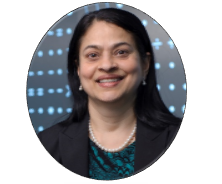
Applications based on optical frequency combs have rapidly grown in diverse areas of science and engineering, including chemical sensing, timekeeping, distance ranging, searching for exoplanets and as a source for wavelength-division multiplexing in data communications. Recent work has shown that chip-based nonlinear photonics offers the prospect of realizing comb devices in highly compact, portable, robust and fully integrated form factors that could make their use ubiquitous for a broad range of environments.  I will describe recent work on Kerr-comb generation and supercontinuum generation for producing  broadband optical frequency combs in chip-based photonic platforms.

AIM Photonics Institute, AIM Academy and materials for waveguide integrated mid-infrared detectors

by
Dr. Anu Agarwal

Massachusetts Institute of Technology, USA

This lecture will focus on polycrystalline lead chalcogenide materials and devices used as mid-infrared photoconductors. Their room temperature processing properties enable integration with back-end Si-CMOS, and the ability to use multi-level layers frees up valuable real-estate on the silicon wafer. Materials include a binary lead chalcogenide (PbTe) for detection upto 3.5 micron wavelength, and ternaries (PbSnTe, PbSeS, PbSeTe) that can detect at longer (upto 6 micron) wavelengths.

Optimization of (i) material properties such as grain size, (ii) electrical properties such as resistivity, mobility and carrier concentration, (iii) optical properties such as responsivity and detectivity, as well as (iv) device design, result in improved photoconductive performance. Photoconductor devices include Resonant Cavity Enhanced (RCE) detector structures that enable an order of magnitude improvement in detectivity, multispectral detectors detect dual IR wavelengths in a single pixel, and MIR detectors integrated with waveguide sensors operating at room temperature.  The high index and mid-IR transparency of PbTe is harnessed to create metalenses, with volume manufacturing as a goal.

The path to workforce competency includes being able to discover disruptive applications, build prototypes and finally transition them to high volume manufacturing.  A glimpse into the negotiation of this path at AIM Photonics Academy will be provided.

An introduction will be made to AIM Photonics Institute, with its world-class CMOS photonics foundry for 300 mm SOI wafers at SUNY-Poly in Albany, as well as its Test Assembly and Packaging (TAP) services offered at a facility in Rochester, NY.

The crossroads of III-V and silicon photonics

by
Prof. Martijn Heck

Eindhoven University of Technology, the Netherlands
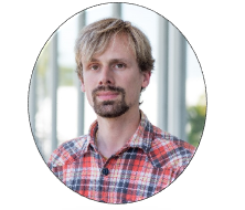
Monolithically integrated platforms, based on silicon, silicon nitride or indium phosphide, i.e., using a single material system, suffer from trade-offs that are necessary to accommodate the fabrication flow. Although such platforms currently have major applications in, e.g., communications and sensing, other, more demanding, applications, might have higher demands. This requires a combination of technologies, taking the “best of both worlds”. Typically, this translates to combining the superior manufacturability and quality of passives of silicon-substrate-based platforms, with lasers, modulators and/or photodetectors in III/V materials. In this lecture I will first review the rationale for doing so. Then I will present an overview of the various state-of-the-art approaches to combine III/Vs with silicon photonics.

Silicon photonics for optical computing

by

Dr. Thomas Van Vaerenbergh

Hewlett Packard Enterprise, Belgium

To keep up with the latency, energy-efficiency and bandwidth needs of future data center and high-performance computing workloads in a cost-efficient way, Hewlett Packard Labs is currently developing silicon photonic interconnects that can hit the required specifications. In this talk, I will illustrate with examples how the recent investments into silicon photonics result in scalable circuits that can be used for a different set of applications: optical computing. Specifically, I will review recent advances in using silicon photonics for machine learning and AI applications, for combinatorial optimization and for digital logic. When introducing these different applications, I will emphasize the importance for our community to compare our emerging silicon photonics solutions both with existing digital electronic solutions and with other emerging technology platforms such as analog electronics or quantum computing. I will conclude the talk by highlighting the remaining challenges for silicon photonics to have a lasting impact in the field of optical computing.

Open-access silicon photonics ecosystem

by

Dr. Abdul Rahim

ePIXfab – Ghent University

This tutorial will provide end-to-end coverage of different silicon photonics technologies and their access routes. The tutorial will also cover the key differentiations of the respective technologies. The latest technological developments made by open-access technologies will be covered in this tutorial.