Silicon Photonics Design Course (3rd Edition)
17th to 21st June 2019 at Ghent University (Ghent, Belgium)
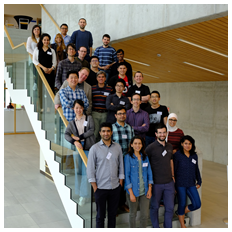
Scope & target Audience
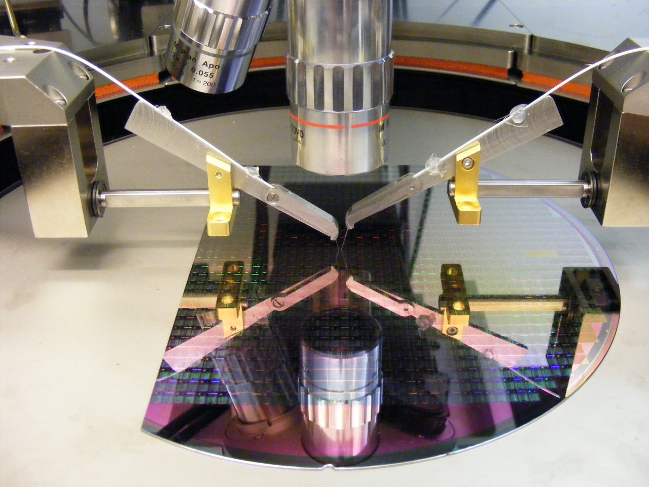
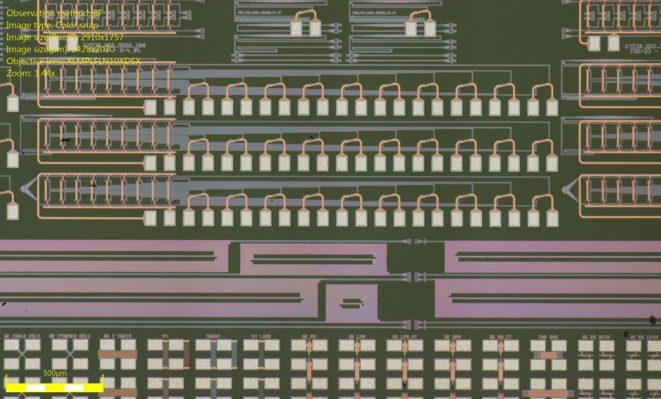
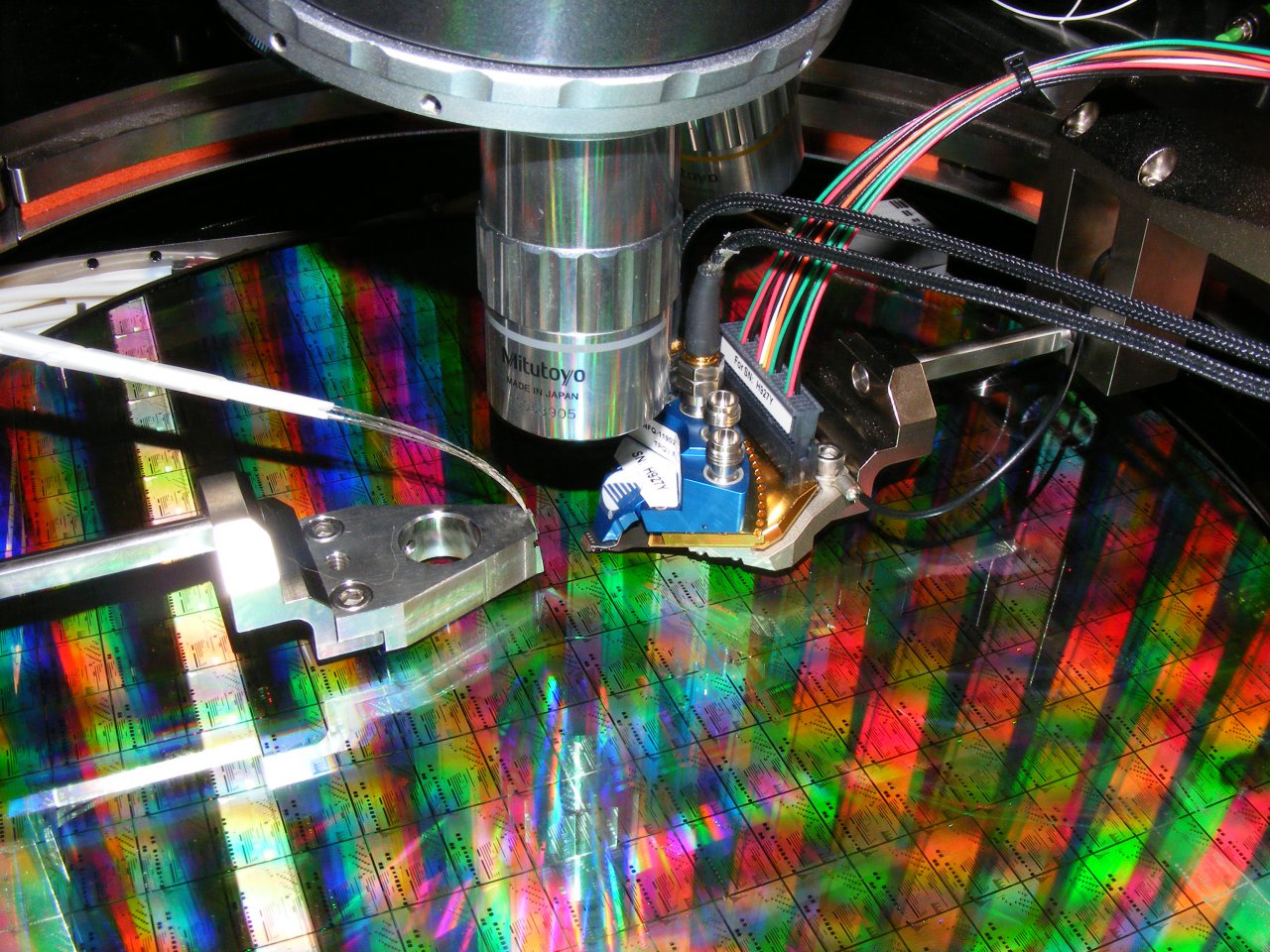
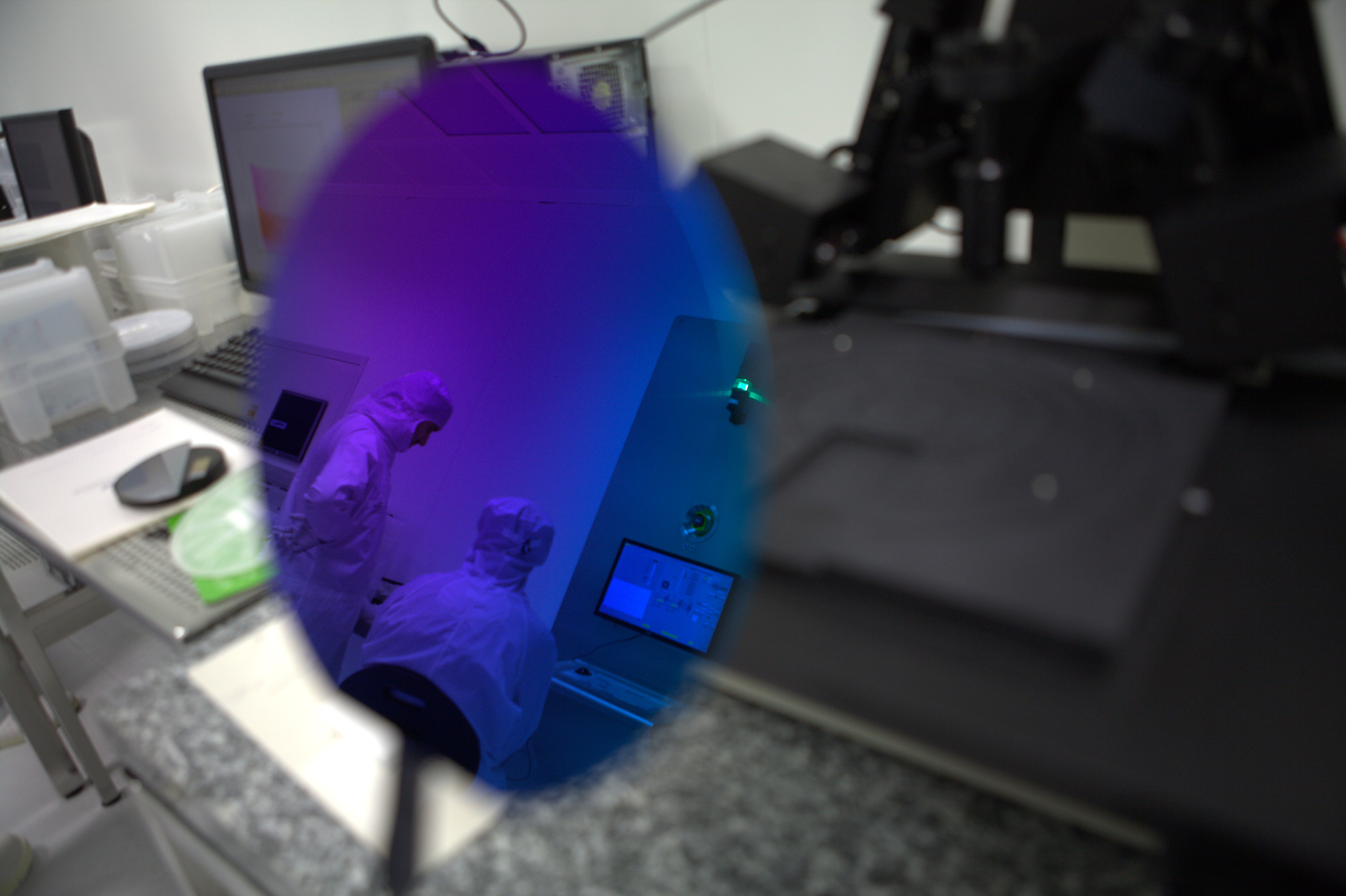
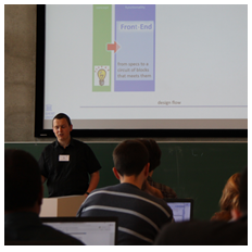
The Specialist Course on Silicon Photonics Design offers a focused, hands-on design course. It is targeted at researchers and engineers with an already fundamental understanding of photonic integrated circuits. The course focused on the process to translate a photonic circuit idea into a working chip, going from schematic design and circuit simulation to layout, routing and interactive design rule checking. As part of the course, the participants get the opportunity to actually tape-out a design that will be fabricated with an e-beam prototyping service and characterized. Based on these results, the design can be improved and submitted to a wafer-scale multi-project-wafer run of which the participants will receive the final chips.

Key features of the course
Gain fundamental understanding of silicon photonics design
Circuits, components, simulation, layout, tape-outs, …
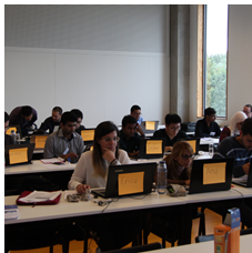
Five days hands-on design lab going all the way from idea to PIC
Get your own design fabricated and tested by measurements
Practical information

Organized by

Supported by