
About imec
Imec aims to be the world-leading R&D and innovation hub in nanoelectronics and digital technologies. As a trusted partner for companies, startups and academia we bring together brilliant minds from all over the world in a creative and stimulating environment. By leveraging our world-class infrastructure and local and global ecosystem of diverse partners across a multitude of industries, we are accelerating progress towards a connected, sustainable future.
Expertise
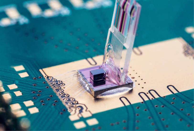
imec’s cutting-edge optical devices are processed at wafer-scale in our in-house 200mm and 300mm CMOS pilot lines. They include high-performance devices for light modulation, switching, coupling, filtering, and detection at data rates of 50GB/s and beyond.
Use qualified reference components from our device library or explore your own custom silicon photonic designs implemented in our platform. Multi-Project Wafer (MPW) runs enable you to cost-efficiently manufacture silicon photonics devices with cutting-edge performance.
imec’s state-of-the-art silicon photonics R&D portfolio covers:
-
- Imec’s iSiPP platform is SOI-based and comes in three distinct flavors:
- iSiPP200: 200mm (8”) full platform
- iSiPP50G: 200mm (8”) simplified platform/flow
- iSiPP300: 300mm (12”) full platform
- Harness the full potential of visible and near-infrared light on integrated circuits with imec’s silicon
nitride (SiN) photonics platform. The platform can be accessed for both photonic integrated circuit
(PIC) prototyping and small volume production.
- Imec’s iSiPP platform is SOI-based and comes in three distinct flavors: