About CMP
CMP (Circuits Multi-Projets) is a nonprofit Multi-Project Wafer (MPW) service organization in ICs, Photonics, 3D-ICs and MEMS for prototyping and low volume production. CMP enables cost effective prototypes fabrication on industrial processes and offers technical expertise in providing MPW and related services for Universities, Research Laboratories and Industrial companies. CMP distributes design rules and design kits for each technology free of charge and supports several CAD software tools for both Industrials and Academics. Since 1981, more than 1000 Institutions from 70 countries have been served, more than 8000 projects have been prototyped, and over 70 different technologies have been interfaced.
Expertise
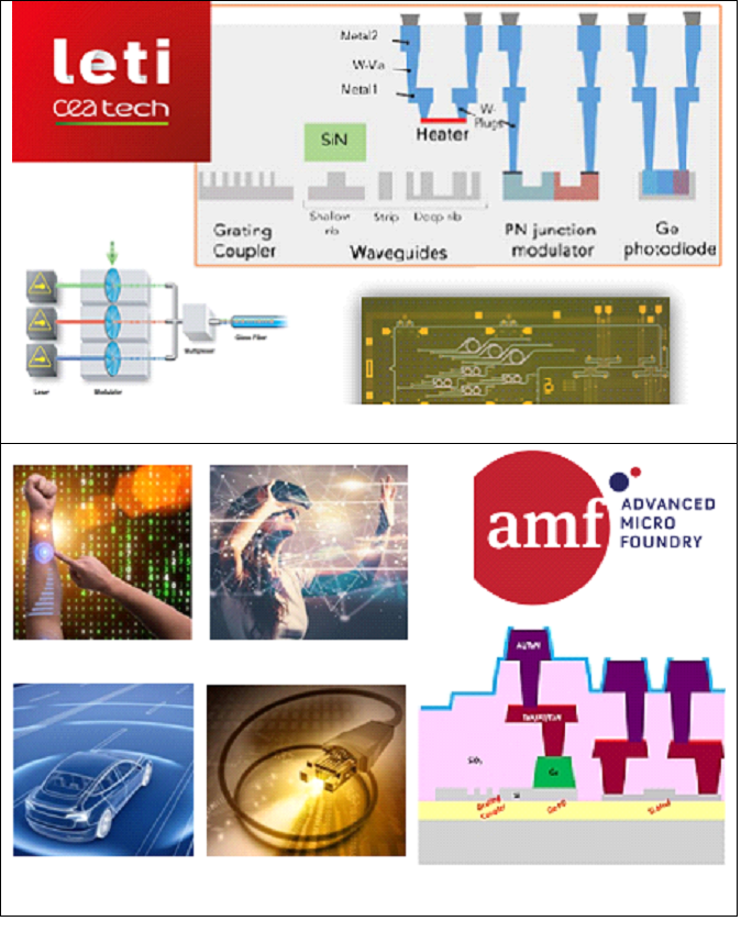
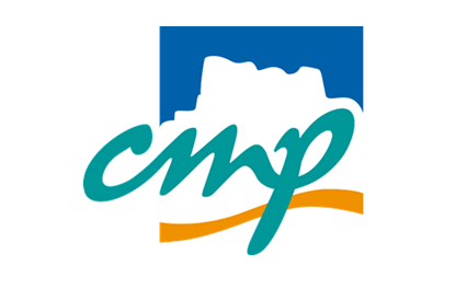
CMP offers access to two silicon photonics technologies: from the French RTO CEA-LETI, dedicated to research and development addressing application areas such as Communication, Computing and Optical sensing, and from the Singaporean founder AMF, more oriented towards Interconnects and Optical sensing and high volume production. Both are based on an SOI platform and have a wide range of active (modulator, photodetector, etc.) and passive (waveguide, coupler, mode adapter, etc.) components. They allow post-process treatments to be carried out (like bump deposition for example) and are available with the main design tools on the market (Cadence, Mentor Graphics and Synopsys).